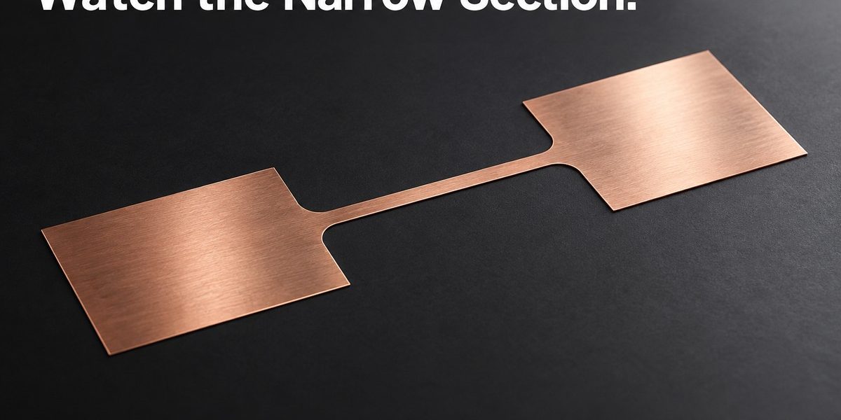
The wide copper pads at either end can make a part look generous. The short narrow section between them may still dominate its electrical and thermal behavior.
The minimum usable width of an etched copper path cannot be chosen from etching capability alone. The finished cross-section, current waveform, allowable temperature rise and heat removal conditions all matter. A manufacturable neck is not automatically a suitable conductor.

Start with the section that carries the current
For a uniform straight conductor at a specified temperature, resistance follows R = ρL/A: resistivity multiplied by length, divided by cross-sectional area. If the thickness and length stay fixed, reducing width reduces area and raises resistance. Power dissipated at a given current follows P = I²R.
These relationships explain why a short constriction deserves attention. They do not produce a universal current rating. Temperature changes resistivity, and the real assembly may remove heat unevenly. A conductor attached to a substantial metal terminal has a different thermal environment from the same geometry suspended between insulating supports.
The drawn width is not the whole cross-section
A sheet-metal outline gives a plan view. The etched edge profile adds a through-thickness shape, so treating every path as a perfect rectangular cross-section can introduce an error where dimensions are small. Identify the section relevant to the electrical model and compare it with the manufactured geometry.
Smooth transitions can also be worth evaluating around a neck, but a large fillet is not a substitute for adequate cross-section. Nearby return conductors, connections and switching conditions become relevant when frequency effects matter.
DC and switching operation ask different questions
Siemens’ September 11, 2026 Simcenter Flux article discusses parasitic extraction from DC to high frequency. For a patterned copper part, the useful implication is that a DC resistance check and a model of switching behavior serve different purposes.
Preserve the current-path geometry and neighboring connections in the model used for electrical evaluation. An isolated outline can leave out the return path that helps determine inductance. Validate temperature rise in the intended mounting arrangement rather than assigning a rating from a photograph.
For a XINKETCHING copper etching inquiry, provide the alloy, sheet thickness and the functional narrow section. Explain whether the design needs a simple resistance target or a wider electrical assessment. That separates what the etching drawing can control from what the complete circuit must prove.
Related engineering reading: metal etching process and DFM guide; thin thermal layers; shield openings and seams.
References: Siemens, From DC to High Frequency: Parasitic Extraction in Simcenter Flux (2026-09-11).

- What Can a Pilot Lot Actually Prove About Etched-Part Repeatability? - October 9, 2026
- How Much Open Area Remains After an Acoustic Mesh Is Assembled? - October 8, 2026
- How Do You Compare Etched Prototypes Without Losing Track of the Design? - October 7, 2026