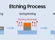
Etching technology is a cornerstone of modern electronics manufacturing, enabling the precise removal of material to create intricate patterns on substrates. Divided into wet etching (using liquid chemicals) and dry etching (using plasma or reactive ions), this process is vital for miniaturization and functionality in electronic devices. Below, we explore its diverse applications across industries.
1. Semiconductor Manufacturing
Etching is indispensable in fabricating integrated circuits (ICs) and microprocessors.
- Transistors and Interconnects : Photolithography defines patterns on silicon wafers, followed by dry etching ( e.g., reactive ion etching) to carve nanoscale features. This creates transistors, gates, and interconnects, adhering to Moore’s Law by enabling smaller nodes (e.g., 5nm in Apple’s M1 chips).
- 3D NAND Flash Memory: Deep reactive ion etching (DRIE) creates high-aspect-ratio vertical memory cells, boosting storage density in devices like SSDs.
2. Printed Circuit Boards (PCBs)
Etching shapes conductive pathways in PCBs:
- Subtractive Process: Copper-clad laminates are masked with photoresist, and wet etching (using ferric chloride) removes excess copper, forming traces. Laser-direct imaging (LDI) enhances precision for high-density interconnects in smartphones and laptops.
3. Displays (LCD/OLED)
- Thin-Film Transistors (TFTs): Dry etching defines TFT arrays on glass substrates for LCDs, crucial for pixel switching in TVs and monitors.
- OLED Pixel Patterning: Fine metal mask ( FMM) etching creates subpixel structures in Samsung’s AMOLED screens, enabling vibrant colors.
4. Microelectromechanical Systems (MEMS)
MEMS devices in sensors and actuators rely on etching:
- Inertial Sensors: DRIE etches silicon to create accelerometers and gyroscopes in iPhones and automotive airbags.
- Microphones : Bosch process etching forms capacitive diaphragms in MEMS mics ( e.g., Apple’s AirPods).
5. Advanced Packaging
- Through-Silicon Vias (TSVs): DRIE drills vertical channels in 3D ICs, connecting stacked dies in AMD’s processors for faster data transfer.
- Fan-Out Wafer-Level Packaging (FOWLP): Etching redistributes interconnects, enabling compact designs in wearables.
6. Flexible and Wearable Electronics
- Flexible PCBs : Wet etching patterns copper on polyimide films for bendable circuits in Samsung’s Galaxy Fold.
- Stretchable Sensors : Laser etching creates serpentine traces for health monitors like Fitbit.
7. Microfluidics and Biomedical Devices
- Lab-on-a-Chip: Isotropic wet etching (HF acid) carves microchannels in glass for portable DNA analyzers (e.g., Illumina’s sequencers).
- Implantables : Etched titanium housings protect pacemakers from corrosion.
8. Photovoltaics
- Anti-Reflective Texturing : Chemical etching textures silicon surfaces in solar panels ( e.g., SunPower cells), boosting efficiency by 20%.
9. Nanotechnology and Quantum Computing
- Nanowires and Quantum Dots : Atomic layer etching ( ALE) tailors nanostructures for Intel’s quantum dot transistors.
- 2D Materials: Plasma etching patterns graphene for ultra-fast RF transistors in 6G research.
10. Quality Control and Failure Analysis
- Cross-Sectioning: Focused ion beam (FIB) etching inspects chip layers for defects, ensuring reliability in automotive ICs.
11. Emerging Applications
- Stretchable Displays: Laser ablation etches silver nanowire grids for foldable OLEDs.
- Eco-Friendly Etching: Transition to dry etching reduces hazardous waste, aligning with EU’s RoHS directives.
Future Trends and Environmental Impact
Advancements in atomic-scale etching and AI-driven process control promise sub-1nm features for next-gen chips. Meanwhile, greener chemistries (e.g., water-based etchants) mitigate environmental risks. As electronics shrink and diversify, etching remains pivotal, bridging innovation with sustainability.
Conclusion
From powering smartphones to enabling quantum leaps in computing, etching technology underpins the electronics landscape. Its evolution continues to drive progress, ensuring devices are faster, smaller, and more efficient while addressing ecological challenges.

- Etching Cost Calculator - June 14, 2026
- Surface Area Calculator - May 24, 2026
- Etch Rate Calculator - May 24, 2026