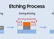
In microfabrication and semiconductor manufacturing, the anti-etching layer ( or etch mask) is critical for selectively protecting regions of a substrate during etching. This layer must meet stringent requirements to ensure precise pattern transfer, durability, and compatibility with complex processes. Below, we explore the key requirements for effective anti-etching layers, material considerations, and process integration challenges.
1. Chemical Resistance
The mask must resist the specific etchant (wet or dry) used:
- Wet Etching: Resistance to acids ( e.g., HF, HNO₃) or bases (e.g., KOH). For example, silicon nitride masks are used with KOH for silicon etching.
- Dry Etching : Resistance to reactive ions ( e.g., CF₄/O₂ plasma) and physical sputtering. Hard masks like SiO₂ or metal (Cr, Al) are preferred for plasma environments.
Material Example: Photoresists may degrade in aggressive plasmas, necessitating hard masks for deep reactive ion etching (DRIE).
2. Adhesion to Substrate
Poor adhesion causes undercutting or delamination. Solutions include:
- Surface Pretreatment : Cleaning with O₂ plasma or using adhesion promoters like HMDS for photoresists on silicon.
- Stress Management: Low intrinsic stress in deposited masks (e.g., CVD SiO₂) prevents peeling.
3. Thickness and Uniformity
- Thickness: Balances durability and resolution. Thin masks (<1 µm) suit high-resolution lithography, while thicker masks (>5 µm) protect during prolonged etching.
- Uniformity: Spin-coated photoresists or ALD/CVD-deposited hard masks ensure consistent protection. Non-uniform layers lead to uneven etching.
4. Thermal Stability
High-temperature processes (e.g., plasma etching) require masks that withstand heat without deforming. Polyimide resists tolerate up to 400°C, whereas standard photoresists degrade above 150°C.
5. Resolution and Patterning Compatibility
- High-Resolution Patterning: Advanced lithography (EUV, e-beam) demands masks with fine grain structure. Chemically amplified resists (CARs) enable sub-10 nm features.
- Edge Acuity: Minimal swelling or roughness during development ensures sharp features.
6. Selectivity
High selectivity (substrate etch rate >> mask etch rate) is critical. For example:
- SiO₂ Masks: Selectivity >100:1 in DRIE silicon etching.
- Metal Masks: Used for high-selectivity plasma etching of dielectrics.
7. Ease of Removal
Post-etch removal must avoid substrate damage:
- Photoresists: Stripped via solvents (acetone) or O₂ plasma ashing.
- Hard Masks: Removed with selective wet etchants (e.g., BOE for SiO₂) or dry etching.
8. Process Compatibility
- Multi-Step Etching: Compatibility with sequential etchants (e.g. , SiO₂ masks for Si etching followed by metal etching) .
- Integration with Deposition: Masks must not react during subsequent CVD/PVD steps.
9. Environmental and Safety Considerations
- Toxicity: Avoid hazardous materials like Cr in favor of safer alternatives (e.g., TiN).
- Waste Disposal: Photoresist strippers containing NMP require specialized handling.
Material Options
| Mask Type | Materials | Applications |
|---|---|---|
| Photoresist | DNQ-Novolac, SU-8 | Optical lithography, MEMS |
| Hard Mask | SiO₂, Si₃N₄, TiN | Plasma etching, high-aspect-ratio features |
| Metal Mask | Cr, Al, Ni | High-selectivity dry etching |
Conclusion
The anti-etching layer is a cornerstone of successful etching processes, requiring careful balancing of chemical, thermal, and mechanical properties. Material selection depends on the etching method, substrate, and desired resolution. Advances in mask materials (e.g., carbon-based hard masks) and deposition techniques continue to push the boundaries of nanofabrication, enabling smaller features and higher device densities.

- Etching Cost Calculator - June 14, 2026
- Surface Area Calculator - May 24, 2026
- Etch Rate Calculator - May 24, 2026