Photo metal etching, also known as photochemical etching or photochemical machining ( PCM) , is a precision manufacturing process that transforms metal sheets into intricate components using controlled chemical reactions. Unlike mechanical methods such as laser cutting or stamping, this technique eliminates mechanical stress and heat distortion, making it ideal for producing high-tolerance, burr-free parts. Our service specializes in delivering custom solutions across industries, combining advanced technology with expert craftsmanship.
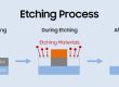
The Photo Metal Etching Process: Step-by-Step
- Material Preparation
- Metals are cleaned to remove contaminants, ensuring optimal adhesion of the photoresist.
- Photoresist Application
- A light-sensitive polymer (photoresist) is laminated onto the metal surface.
- UV Exposure
- The coated metal is exposed to UV light through a phototool (film mask) that defines the part’s design. Unexposed areas remain soluble.
- Development
- The panel is immersed in a developer solution, dissolving unexposed photoresist to reveal bare metal in the desired pattern.
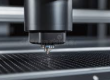
- Chemical Etching
- The metal is sprayed with an etchant (e.g., ferric chloride), which dissolves exposed areas to create precise features.
- Photoresist Stripping
- Remaining resist is removed, leaving a clean, finished part.
- Post-Processing
- Optional steps include plating, annealing, or forming to meet specific requirements.
Materials Compatible with Our Service
We work with a wide range of metals, each chosen for unique properties:
- Stainless Steel : Corrosion resistance, durability ( e.g., medical instruments).
- Copper & Alloys: Superior conductivity (e.g., electrical contacts).
- Aluminum: Lightweight, thermal management (e.g. , heat sinks) .
- Nickel Alloys (Inconel, Hastelloy): High-temperature performance (e.g., aerospace components).
- Brass: Aesthetic appeal and machinability (e.g., decorative panels).
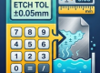
Thickness Range: 0.01 mm to 1.5 mm, with tolerances as tight as ±0.025 mm.
Advantages of Photo Metal Etching
- Precision: Achieve complex geometries, micro-sized features, and sharp edges without tool wear.
- Stress-Free: No thermal or mechanical distortion, preserving material integrity.
- Cost-Efficiency: Low setup costs and no hard tooling, ideal for prototypes and high-volume runs.
- Speed: Rapid turnaround (days vs. weeks for stamped parts).
- Scalability: Seamlessly transition from prototypes to mass production.
Comparison to Traditional Methods:
- Laser Cutting : Risk of heat-affected zones; limited to thicker materials.
- Stamping: High tooling costs and lead times; less design flexibility.
Industry Applications
- Electronics: EMI/RFI shields, lead frames, and connectors.
- Aerospace: Lightweight turbine blades, fuel cell components.
- Medical: Surgical tools, implantable devices, and sensor grids.
- Automotive: Fuel injector shims, ABS system parts.
- Industrial : Filters, sieves, and encoder discs.
Why Choose Our Service? Key Considerations
- Material Expertise: Decades of experience selecting optimal alloys for your application.
- Quality Assurance: ISO-certified processes, including precision inspection (CMM, optical comparators).
- Capacity: Support for both R&D projects and large-scale production.
- Sustainability: Eco-friendly etchant recycling and waste management.
- Added Value: Secondary services like plating, annealing, and CNC forming.
Design Guidelines
- Minimum Feature Size: 0.1 mm (dependent on material thickness).
- Tolerances: Typically ±10% of material thickness.
- File Preparation: Vector-based formats (DXF, DWG) with clear cutlines.
Conclusion
Our photo metal etching service offers unmatched precision, versatility, and efficiency for industries demanding high-performance metal components. By leveraging advanced photochemical technology and a customer-centric approach, we deliver solutions that meet stringent quality standards while reducing costs and lead times.
Contact Us Today to discuss your project requirements and experience the benefits of cutting-edge photo etching tailored to your needs.

- Etching Cost Calculator - June 14, 2026
- Surface Area Calculator - May 24, 2026
- Etch Rate Calculator - May 24, 2026