Etching is critical in the modern electronics industry, where precision and miniaturization are paramount. The global market for etching technology is projected to reach billions of dollars by the end of this decade, underscoring its importance in producing electronic devices. Etching, a process of removing material from a substrate to create intricate patterns, is indispensable in manufacturing circuit boards and electronic components.
This article will explore the various types of etching, including chemical, plasma, and laser etching, and examine how these processes contribute to creating essential electronic components. By understanding the role of etching, we can appreciate its impact on the electronics industry’s efficiency, functionality, and innovation.
Understanding Etching
Etching is a subtractive manufacturing process that involves removing material from a substrate to create specific patterns or designs. This technique is fundamental in the electronics industry, enabling the precise fabrication of intricate circuits and components essential for modern devices.
Types of Etching
Chemical Etching
In this method, acids or other chemical agents dissolve material from the substrate. The process typically involves applying a resist to protect areas that should remain intact while the exposed regions are etched away. Chemical etching is widely used for manufacturing printed circuit boards ( PCBs) due to its ability to produce fine details on metal surfaces like copper.
Plasma Etching
Plasma etching employs ionized gases, or plasma, to remove material from a substrate. This technique is essential in semiconductor fabrication, which is used to etch tiny features on silicon wafers. Plasma etching offers high precision and is necessary to create the minute structures in integrated circuits.
Laser Etching
Lasers provide a highly accurate means of etching by vaporizing material with focused light beams. Laser etching is used for marking and identification purposes on various electronic components, such as adding serial numbers or logos. It is also used in cases where traditional methods might damage sensitive materials.
Materials Used
The most common materials subjected to etching include copper for PCBs, silicon for semiconductor devices, and various metals or polymers for other electronic components. These materials are selected based on their conductivity, durability, and compatibility with specific etching techniques.
The Role of Etching in Circuit Board Manufacturing
Printed Circuit Boards (PCBs)
Printed Circuit Boards (PCBs) are the backbone of virtually all electronic devices, providing a physical platform for the electrical connections between various components. PCBs enable the efficient and compact arrangement of circuits, making them essential for modern electronics, from smartphones to industrial machinery.
Etching Process in PCB Production
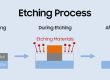
The production of PCBs relies heavily on etching to create the necessary circuit patterns on the board’s surface. The process begins with applying a photoresist, a light-sensitive material, onto the copper-clad substrate. The photoresist is then exposed to UV light through a photomask defining the desired circuit pattern. The exposed areas harden, while the unexposed regions remain soft and are washed away. The board is then subjected to an etching solution, typically an acid, which removes the unprotected copper, leaving behind the intricate circuit patterns. Finally, the remaining resist is stripped away, revealing the etched circuit.
Precision and Complexity
Etching allows for the creation of exact and complex circuit patterns that are crucial for modern electronic functionality. As devices become more compact, the ability to etch fine lines and spaces on PCBs is increasingly essential for maintaining performance and reliability.
Surface Mount Technology (SMT)
Etching also plays a critical role in Surface Mount Technology (SMT), which is used to mount electronic components directly onto the surface of PCBs. Through etching, solder pads and other necessary features are created, allowing for the precise placement and connection of components. This process enhances the efficiency and miniaturization of electronic devices.
Etching in Semiconductor Fabrication
Semiconductor Manufacturing
In semiconductor manufacturing, etching is a vital process that defines the intricate features of microchips and other electronic components. These components, often made from silicon wafers, are the foundation for all semiconductor devices, including processors, memory chips, and sensors. Etching is particularly crucial for defining the minute structures, such as transistors, that enable the complex functionality of these devices.
Dry vs. Wet Etching
Two primary etching methods are used in semiconductor fabrication: dry etching and wet etching.
Dry Etching
This method involves using plasma or reactive gases to remove material from the wafer. Dry etching offers greater precision and control, making it ideal for creating the fine features required in modern microchips. It is beneficial for anisotropic etching, where the etching rate is directionally dependent, allowing for the creation of vertical sidewalls in the material.
Wet Etching
In contrast, wet etching uses liquid chemicals to dissolve materials. While less precise than dry etching, it is more straightforward and cost-effective, making it suitable for processes where high precision is not as critical. Wet etching is often used for isotropic etching, where the material is removed uniformly in all directions.
Microelectromechanical Systems (MEMS)
Etching is also fundamental in producing Microelectromechanical Systems (MEMS), tiny devices that combine electrical and mechanical components. These systems are integral to various applications, including sensors, actuators, and microprocessors. Etching enables the precise shaping and structuring of MEMS components, allowing for miniaturization and integration into electronic systems.
Advancements in Etching Techniques
Recent advancements in etching technology have significantly improved the efficiency and precision of semiconductor fabrication. Innovations such as atomic layer etching ( ALE) allow for even finer control over material removal, enabling the production of increasingly smaller and more complex semiconductor devices. These advancements are crucial as the industry continues to push the boundaries of miniaturization and performance in electronic components.
Etching in Electronic Components
Connectors and Contacts
Etching plays a crucial role in creating connectors, contacts, and other small components that are integral to the functionality of electronic devices. These elements are responsible for ensuring reliable electrical connections between different parts of a circuit. Through etching, manufacturers can produce connectors and contacts with high precision, enabling them to meet the exacting standards required for modern electronics. This precision ensures that the components fit perfectly within the compact spaces of electronic devices, contributing to overall device reliability.
Aesthetic and Functional Markings
Etching is also used to add both functional and aesthetic markings to electronic components. This includes serial numbers, logos, barcodes, and other identification marks essential for product tracking, authentication, and branding. Laser etching, in particular, allows for creating sharp, durable markings that can withstand the rigors of everyday use. These markings not only enhance the functionality of the components but also contribute to the brand identity of the electronic devices.
Customization and Miniaturization
As electronic devices continue shrinking, the demand for customized and miniaturized components has grown. Etching facilitates this trend by enabling the production of highly customized components that can be tailored to specific applications. Whether it’s creating uniquely shaped connectors or intricate circuit patterns, etching allows manufacturers to meet the diverse needs of modern technology, ensuring that electronic devices remain compact, efficient, and versatile.
Challenges and Future Trends
Material Limitations
As electronics become more complex, the variety of materials used in their construction also increases. Etching different materials, especially those more resistant to traditional etching processes, presents significant challenges. The need to etch multiple layers of different materials simultaneously adds to the complexity, requiring more advanced techniques and equipment.
Environmental Concerns
Chemical etching often involves using hazardous substances, which can have negative environmental impacts if not appropriately managed. The industry is increasingly focused on reducing these impacts by developing more sustainable etching methods, improving waste management, and minimizing the use of harmful chemicals.
Future Trends
Nano-Etching
The future of electronics is leaning towards further miniaturization, and nano-etching techniques are at the forefront of this trend. Nano-etching allows for the creation of excellent features at the nanometer scale, which is essential for the next generation of microelectronics, including quantum computing and advanced sensors. This technique promises to push the boundaries of what’s possible in electronic design.
Green Etching Technologies
With growing environmental awareness, greener etching technologies are gaining momentum. Dry etching, which uses less harmful chemicals, is becoming more popular as a sustainable alternative to traditional chemical etching. Additionally, innovations in etching processes that reduce energy consumption and waste generation will likely shape the industry’s future.
Conclusion
Etching is a vital process in electronics, essential for producing circuit boards, semiconductors, and intricate components needed for modern technology. As the industry evolves, advancements in nano-etching and eco-friendly methods will drive innovation. Staying informed on these developments is critical to staying competitive.
Xinketching stands out as a leading manufacturer specializing in etched hardware, dedicated to bringing your projects to life with exceptional metal etching services. Experience the perfect blend of precision, quality, and innovation. Connect with us today to transform your ideas into finely crafted metal solutions. Let’s collaborate to make your vision a reality.

- Etching Cost Calculator - June 14, 2026
- Surface Area Calculator - May 24, 2026
- Etch Rate Calculator - May 24, 2026