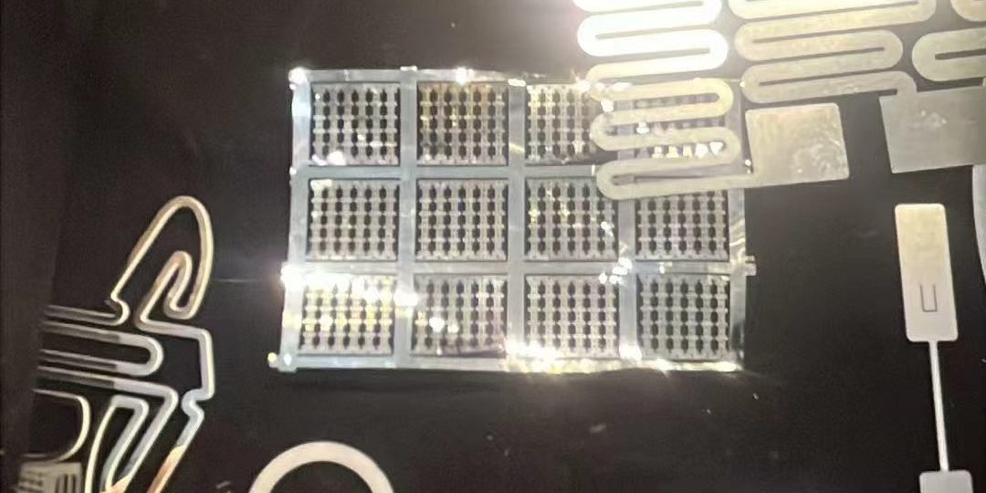
Battery contacts, spring clips and thin-gauge busbar parts are flat, burr-sensitive and geometry-rich — which is why cell and module makers increasingly have them photo-etched rather than stamped. Xinketching is a precision photochemical etching manufacturer in Dongguan, China, producing flat etched metal parts since 2005. This article covers the etched parts that sit between cells and circuits in EV packs and stationary storage: which of them etching suits, in which materials and gauges, and where a busbar stops being an etching job.
Answer capsule: what etching is used for in a battery pack
- Cell contact tabs and connector plates — flat copper or nickel parts that link cells to the pack’s circuitry, with holes, slots and locating features cut in the same pass as the outline.
- Spring contacts and clips — thin-gauge parts whose contact fingers are etched flat, with half-etched fold lines marking exactly where each finger bends.
- Thin-gauge busbar and distribution parts — flat current-carrying plates up to 2.5 mm thick for cell-level and module-level interconnects, sensing plates and distribution links inside the pack.
- Why etched, not stamped: no hard tooling, burr-free edges next to separators and cell casings, and identical geometry from the first prototype to production on the same digital artwork.
Specifications
- Materials: copper, brass (standard grade H62 / UNS C27200; other copper-alloy grades sourced to the grade specified on your drawing), nickel, stainless steel, titanium — we do not etch aluminium
- Thickness range: 0.05–2.5 mm — gauges 0.05, 0.08, 0.1, 0.12, 0.15, 0.2, 0.25, 0.3, 0.4 and 0.5 mm are stocked; above 0.5 mm up to 2.5 mm is sourced per order
- Dimensional tolerance: ±10% of material thickness (e.g. ±0.02 mm on 0.2 mm stock, ±0.05 mm on 0.5 mm stock); raw-stock thickness tolerance ±0.02 mm
- Minimum through-features: ≈ material thickness (design rule ≈ 0.8–1.2× thickness)
- Half-etched features: fold lines, recesses and marks at ≈50–75% of thickness, depth control ±0.05 mm
- Finishing: passivation in-house; all plating types available via qualified partners (tin, nickel and other contact finishes are partner-applied, never claimed as in-house); bending/forming and secondary stamping also via partners
- Format: flat sheets only, no coil/reel-to-reel; maximum single sheet 600 × 1,450 mm for material 0.5 mm and above
- Lead times and order terms: samples 3–5 days, production 7–10 days; no minimum order quantity, minimum order charge US$100; FOB
- Quality documents: material test certificate with per-run material batch traceability; PPAP Level 3 supported; IMDS data available; NDAs on request
The parts, one by one
Contact tabs and connector plates are the volume item. They are flat, they carry many small features — weld windows, locating holes, polarity marks — and they sit against cell casings and separators, where a stamping burr is not a cosmetic defect but a puncture risk. Etching produces them burr-free and stress-free, and because the tooling is digital, a tab geometry can be revised in days while a pack design is still moving, then carried unchanged into production. Spring contacts add one etching-specific trick: a half-etched groove along each fold line sets the bend position precisely on every part; the bending itself is a partner operation, and the groove is what makes it repeatable. Busbar parts are where the gauge range matters — etched busbars make sense in the 0.3–2.5 mm band, for module interconnects, end plates and sensing links whose outlines are too complex, or volumes too young, for a die. Where a contact surface needs tin or nickel plating, the full range of finishes is available through our qualified finishing partners, as set out on the Automotive Precision Etched Parts page.
Designing for current, not just for shape
An etched busbar is still a conductor, and two drawing decisions dominate. The first is cross-section: current capacity follows the metal cross-section, so thickness and the narrowest land width on the current path set the rating — a necked-down section drawn for packaging reasons is a hot spot, and should be sized as deliberately as the terminals. The second is the feature floor: holes and slots cannot be etched reliably much below the material thickness, so a 1.5 mm busbar cannot carry 0.5 mm perforations, and terminal hole patterns should be checked against the gauge before the print is released. Material choice follows the same engineering: copper for conductivity, nickel where corrosion behaviour and weldability lead, brass (standard stocked grade H62) for lower-current connector parts — the trade-offs are worked through in our post on etching copper and brass.
Where etching stops being the right process
Honesty about the boundary saves both sides a quotation cycle. Main traction busbars in thick bar — well above our 2.5 mm ceiling — belong to stamping, CNC or bar stock, not etching. Very high volumes of a frozen, simple outline will eventually favour a progressive die on unit cost, though etching remains the fastest route to validated parts while the design settles. And plating, bending and welded assembly are downstream steps, applied by qualified partners and stated as such on the quotation. Programmes that need the documentation set behind the part — PPAP Level 3, IMDS entries, material certificates tied to the production batch — are the ones we are set up for; the same discipline applies to the etched lead frames we supply into electronics production.
FAQ
Can you etch a complete busbar assembly?
We etch the flat parts — plates, tabs, links — up to 2.5 mm thick. Insulation, lamination, bending and assembly are separate steps; bending and plating are available via our partners, and we will tell you at quotation exactly which steps sit where.
Which plating can the contacts have?
All common contact finishes, including tin and nickel plating, applied by qualified finishing partners. Passivation of stainless parts is done in-house.
How fast can a new contact design be sampled?
Samples in 3–5 days from artwork approval, on the same digital tooling that later runs production — there is no die to cut, so the sampled part is the production part.
What do you need to quote?
The drawing or DXF, material and thickness, quantities for samples and production, and any plating or documentation requirements (PPAP, IMDS). NDAs are signed on request before drawings change hands.
Send us the drawing
Xinketching etches battery contacts, spring clips and thin-gauge busbar parts in copper, brass, nickel and stainless steel from 0.05 to 2.5 mm, with samples in 3–5 days, production in 7–10 days, no minimum order quantity and a US$100 minimum order charge. Send the drawing through our contact page or to sales@xinketching.com, and we will confirm the gauge, the feature floor and the plating route against your print.

- What Does a 770 W/cm² GPU Hotspot Mean for the Etched Copper Flow Layer? - November 22, 2026
- Photo-Etched Precision Medical Metal Components: Micro-Needles, Lancets and Microfluidic Parts - November 21, 2026
- Custom Lead Frame Etching for IC Packaging: Photo-Etched vs Stamped Lead Frames - November 18, 2026