Photochemical machining (PCM), also called photo chemical etching or photo etching, is a subtractive sheet-metal process that uses photoresist and controlled chemical etching to produce thin, flat precision parts. It is especially useful when a design contains many holes, slots, spring features, screens or complex profiles that would make hard tooling expensive or introduce burrs and mechanical stress.
For engineers, the key question is not whether PCM is universally better than stamping, laser cutting or CNC machining. It is whether the part geometry, material thickness, tolerance, volume and edge requirements fit the process window. PCM is strongest for thin metal parts, rapid design changes and geometries where tooling cost or thermal/mechanical effects matter.
This guide explains the process, materials, tolerance drivers, applications and practical DFM considerations so you can decide when photochemical machining is the right manufacturing method.
History and Evolution of Photochemical Machining
In the 1960s, photochemical machining (PCM) emerged as a spinoff from the printed circuit board ( PCB) sector. PCM was first employed to create complex PCBs with extreme precision, but it soon became known for its remarkable accuracy in producing complex metal parts.
Technological developments in photoresist materials, etchants, and imaging have been directly linked to the growth of PCM. The earliest PCM methods used simple etchants and photo tools. However, PCM developed into a highly accurate and adaptable production process with the advent of specialized etchants and more advanced photo tools with finer resolutions.
The capabilities of PCM have been greatly expanded by critical technological developments, such as UV-sensitive photoresists and computer-aided design (CAD) software for photo tool production. Thanks to these developments, manufacturers can now create products with complex features, precise geometries, and tight tolerances that were previously difficult to do using conventional machining techniques.
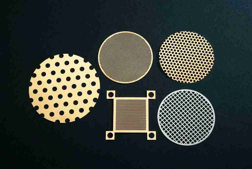
PCM is a significant force behind innovation in several industries, including electronics, medical devices, automotive, and aerospace. Due to its capacity to manufacture a wide range of components, from semiconductor lead frames and RF/microwave circuits to small screens and meshes, is a favored option with the least amount of material waste. By allowing engineers and designers to push the limits of what is feasible in manufacturing metal components, PCM continues to spur innovation.

Process Overview of Photochemical Machining
A precise set of procedures called photochemical machining (PCM) turns a design concept into a finished metal product. An outline of the PCM process is provided below, emphasizing its essential components and the significance of accuracy and precision:
Design and Preparation
To start the process, the part to be made is designed using computer-aided design (CAD) software. The digital image used for the photo tool is then created from the design.
Phototool Creation
The digital image of the part is printed onto dimensionally stable and optically clear photographic film to create a photo tool. This photo tool comprises two sheets that display negative photographs of the component, with black areas denoting places that need to be etched and precise portions depicting the part’s shape.
Material Preparation
After cleaning, a UV-sensitive photoresist is applied to both sides of the metal sheet or plate that has to be etched. During the etching process, this photoresist acts as a shielding layer.
Exposure and Development
The coated metal sheet is positioned between the photo tool’s two sheets and vacuumed to guarantee good contact. The assembly is then subjected to UV light, which causes the photoresist in the phototool’s clear sections to solidify. Following exposure, the sheet is developed, leaving the portions to be etched and eliminating the photoresist that was not exposed.
Etching
An etchant solution is sprayed onto both sides of the metal sheet using spray nozzles in a multi-chambered machine used for the etching process. The desired portion is left behind while the exposed metal is selectively removed by the etchant, which is frequently an aqueous solution of an acid like ferric chloride.


Post-Etching Processing
The part is cleaned and dried, and any leftover photoresist is removed. Any last details like surface treatments or deburring can be added.
Materials and Equipment
- Photoresists: UV-sensitive coatings that protect the metal during etching.
- Phototools: Transparent films with negative images of the part to be etched.
- Etchants:Chemical solutions that selectively dissolve the exposed metal.
- Etching Machines:Multi-chambered equipment with spray nozzles for precise etchant application.
Precision and Accuracy: PCM methods depend heavily on precision and accuracy to guarantee that the finished components fulfill design parameters. Dimensional faults or flaws in the final pieces might arise from variations or mistakes in the photo tool or etching process. High-quality photo tools, exact exposure and development procedures, and regulated etching conditions are necessary for PCM accuracy and precision.
Advantages of Photochemical Machining
Photochemical machining (PCM) is the method of choice for producing complex metal parts since it has many clear advantages over conventional machining techniques. These are a few of PCM’s main benefits:
Cost-Effectiveness
PCM is incredibly cost-effective, particularly when making complex parts in small to medium quantities. The procedure drastically lowers upfront costs by eliminating the requirement for pricey tooling like dies or molds. Furthermore, PCM reduces material waste by efficiently using raw materials because just the appropriate regions of the metal sheet are etched.
Quick Turnaround Times
PCM’s streamlined tooling process and effective etching capabilities allow for fast development and production cycles. Rapid design iterations and modifications enable quicker product development and time-to-market.
High Precision
Even with complex products, PCM is exceptional at attaining tight tolerances and high precision. Utilizing sophisticated photo tools and carefully calibrated etching procedures guarantees precise and reliable outcomes that meet the design’s requirements.
Versatility
PCM can work with various metals and alloys, such as titanium, copper, brass, aluminum, and stainless steel. Because of its adaptability, PCM may be used in multiple industries, including aerospace, electronics, medical technology, and automotive components.
When it comes to cost-effectiveness for small to medium production runs, speedy prototyping and production turnaround times, high precision even for complex geometries, and versatility in working with different metals and alloys, PCM offers superior capabilities compared to traditional machining methods like stamping, punching, or laser cutting. With these benefits, PCM is positioned as a highly competitive and efficient manufacturing method in the demanding industrial landscape.
Applications of Photochemical Machining
It is widely used in various sectors because photochemical machining (PCM) can manufacture accurate, precise, and detailed metal parts. Let’s examine several important industries and particular instances of PCM-manufactured parts and components:


Electronics Industry
Microelectronics Components
PCM is frequently used to make microelectronic components, including lead frames, connections, and integrated circuit (IC) packages. It is the perfect material for the precise and fine details required to manufacture complex electronic device parts.
EMI/RFI Shields
Electronic equipment must be protected from radio frequency interference (RFI) and electromagnetic interference (EMI). PCM creates EMI/RFI shields to safeguard delicate electronic components with exact patterns and measurements.
Aerospace Industry
Aircraft Components
PCM makes vital parts for the aircraft industry, including heat sinks, brackets, and sensor housings. It can effectively deliver these components’ high precision and lightweight designs.
RF/Microwave Components
Circuits and parts for RF and microwave technology are frequently used in aerospace applications. PCM is used to make these components with exact dimensions and detailed patterns to achieve strict performance requirements.
Medical Device Industry
Implantable Devices
PCM is employed as a component in stents, surgical instruments, and sensor components, among other implantable medical devices. Due to their biocompatibility, medical applications can benefit from PCM-produced parts.
Diagnostic Equipment
PCM is used to produce parts for diagnostic equipment, including MRI coils, ultrasound transducers, and X-ray detectors. This is because PCM can produce intricate features and complex shapes.
Automotive Industry
Fuel System Components
PCM is used to make parts of gasoline systems, including rails, sensors, and injector nozzles. Precision machining is necessary for these parts to function at their best and use the least fuel.
Electronic Control Units (ECUs)
Electronic control units use PCM for engine management, safety features, and networking in automobile systems. Because PCM is highly accurate, these vital components are reliable and functional.
Consumer Electronics Industry
Smartphone Components
PCM produces speaker grilles, camera modules, and antenna housings for cell phones. PCM is perfect for consumer electronics applications because it can create complex designs with little material waste.
Wearable Devices
PCM’s accuracy and adaptability are utilized to make components for wearable electronics, including fitness trackers, smartwatches, and medical wearables.
PCM’s accuracy and adaptability make it indispensable in various industries, allowing for the superior quality and accuracy of a wide range of parts and components to be produced.
Economic Considerations in Photochemical Machining
The many financial benefits that photochemical machining (PCM) provides have led to its widespread use in manufacturing:
Low Tooling Costs
PCM dramatically lowers the upfront investment costs by eliminating the requirement for pricey toolings like dies or molds. Comparatively speaking, PCM photo tools are less expensive than the tooling needed for conventional machining procedures.
Efficient Material Usage
Because PCM only etchs the appropriate portions of the metal sheet, it maximizes material utilization and reduces waste. This lowers the price of raw materials and promotes environmental sustainability.
Scalability
Small to medium manufacturing runs can use PCM without seeing appreciable cost increases. Its scalability gives manufacturers flexibility by making it appropriate for mass production and prototypes.
In terms of cost, PCM is more advantageous than traditional machining methods. For example, costly tooling and increased material waste may be associated with CNC machining or stamping, whereas PCM is more economical in certain situations. PCM’s competitiveness in terms of economic efficiency is further enhanced by its ability to produce complicated parts with high precision and rapid turnaround times.


Challenges and Future Trends in Photochemical Machining
In terms of cost, PCM is more advantageous than traditional machining methods. For example, costly tooling and increased material waste may be associated with CNC machining or stamping, whereas PCM is more economical in certain situations. PCM’s competitiveness in terms of economic efficiency is further enhanced by its ability to produce complicated parts with high precision and rapid turnaround times.
Ongoing research and development efforts are concentrated on advancing PCM technology to address these problems. This covers developments in etchants, process automation, and photoresist materials. Digital imaging and photo tool creation advances aim to improve PCM processes’ accuracy and resolution. Furthermore, combining PCM with additive manufacturing techniques is becoming more popular in creating hybrid manufacturing systems that capitalize on the advantages of both technologies. Through these initiatives, PCM is evolving to become more adaptable, dependable, and affordable for manufacturing applications.
When Photochemical Machining Is a Good Fit
- Thin, flat metal parts with complex profiles, dense holes or slots.
- Designs that may change during prototyping and would make hard tooling expensive.
- Parts where burr-free edges and low mechanical stress are important.
- Applications such as EMI shields, encoder discs, precision shims, filter plates, spring contacts, nozzle/orifice plates and thin flow components.
When Another Process May Be Better
PCM is not the best choice for every part. Thick 3D components, deep pockets, formed features, extremely tight tolerances independent of thickness, or very high-volume simple geometries may be better suited to CNC machining, laser cutting or stamping.
For tolerance planning, see the Chemical Etching Tolerance Calculator. For stainless-steel-specific guidance, see Stainless Steel Etching.
Conclusion
Photochemical machining is most valuable when part geometry, material thickness, tolerance and production volume align with the process. Before choosing the method, review the drawing rather than relying on a generic capability claim. Xinketching can review material grade, thickness, critical dimensions, hole/slot geometry and tolerance requirements to determine whether photo chemical etching is appropriate for the part.
For a current consumer-electronics example, see our foldable phone metal etching guide, covering titanium support plates, micro-patterned holes, precision mesh and thin-metal DFM.

- Etching Titanium: When the Weight or the Chemistry Earns It - October 24, 2026
- Etching Copper and Brass: What Changes vs Stainless Steel - October 23, 2026
- Etching Stainless Steel: 304 vs 316L vs 301 for Etched Parts - October 22, 2026