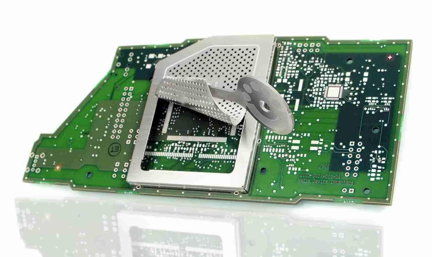
PCB EMI shielding is used to control electromagnetic interference around sensitive circuits, connectors and RF sections. In precision metal manufacturing, photochemical etching is commonly applied to the thin metal shielding parts themselves—such as shielding cans, covers, frames and patterned sheet components—rather than to the PCB substrate.
For these parts, photo etching is valuable when engineers need complex openings, ventilation patterns, tabs, fold lines or multiple design variants without investing in hard tooling. Stainless steel, copper and other conductive sheet metals can be patterned from CAD data and then formed or assembled as required.
This guide explains how photochemical etching supports PCB and electronic EMI shielding, what design factors matter, and when etched shielding is preferable to stamping, laser cutting or other fabrication methods.
Understanding PCB Shielding
PCB shielding serves as a vital defense mechanism, shielding sensitive electronic circuits from the pervasive influence of external electromagnetic radiation. This radiation, known as electromagnetic interference (EMI), can originate from various sources, such as power lines, electronic devices, and wireless communication signals. EMI can infiltrate PCBs without proper shielding, causing signal distortion, data corruption, and device malfunctions.
The impact of EMI on electronic devices is profound, often leading to degraded performance and reliability issues. Common manifestations of EMI include signal noise, voltage spikes, and electromagnetic coupling between adjacent components. In high-frequency applications like wireless communication or medical equipment, EMI can be particularly detrimental, compromising the accuracy and stability of critical functions.
Shielding materials are pivotal in protecting electromagnetic fields from sensitive circuitry. These materials, often composed of conductive metals like copper or aluminum, create a barrier that absorbs or reflects electromagnetic waves, preventing their penetration into PCBs. By confining EMI to external surfaces or dissipating it harmlessly, shielding materials ensure the integrity of electronic signals and the optimal functioning of electronic devices. Thus, understanding the principles of PCB shielding and selecting appropriate shielding materials are essential steps in designing robust and reliable electronic systems.
Photochemical Etching Process
The photochemical etching process is a sophisticated yet highly effective technique for creating precise, intricate shielding patterns on PCB surfaces. It begins with preparing the PCB substrate, typically made of materials like fiberglass or epoxy resin, which serves as the foundation for the shielding structure.
The first step in photochemical etching involves applying a photosensitive mask to the PCB surface. This mask, often composed of a photosensitive polymer or dry film resist, is designed to be selectively exposed to UV light. The mask is laminated onto the substrate, ensuring complete coverage and adhesion.
Next, UV light is used to expose the photosensitive mask through a photo tool or mask that contains the desired shielding pattern. The UV light penetrates the mask in areas where shielding is required, activating the photosensitive material and causing it to change chemically. This exposure creates a stencil-like pattern on the mask, defining the areas to be etched on the PCB surface.
Following exposure, the PCB undergoes a development process where the unexposed areas of the photosensitive mask are dissolved or removed, leaving behind the desired shielding pattern—the exposed portions of the mask act as a protective barrier during the subsequent etching step.
Etching is typically carried out using chemical solutions that selectively dissolve the exposed areas of the PCB substrate, effectively etching away the material and leaving behind the precise shielding pattern. The etching process can be controlled with high precision, ensuring accurate reproduction of complex shielding geometries.
Photochemical etching offers several advantages over traditional methods for creating PCB shielding. It boasts high accuracy, allowing for intricate and delicate details in shielding patterns. The process is also scalable, making it suitable for prototyping and mass production. Additionally, photochemical etching is cost-effective, as it minimizes material waste and reduces the need for extensive tooling compared to mechanical methods. These advantages make photochemical etching a preferred choice for achieving precise and effective PCB shielding.


Types of Shielding Patterns
Photochemical etching enables the creation of various shielding patterns tailored to specific needs in electronic design. Here are three types of shielding patterns achievable through this process:
Continuous Shields
Continuous shields provide uniform coverage over large areas of the PCB surface, creating a consistent barrier against electromagnetic interference (EMI). These shields protect entire circuit sections or sensitive components from external radiation sources.
Intermittent Shields
Intermittent shields feature periodic gaps or openings in the shielding pattern, strategically designed to allow for signal transmission while still providing EMI protection. These shields strike a balance between shielding effectiveness and signal integrity, making them suitable for applications where both are critical.
Selective Shielding for Specific Components
In some cases, specific components or areas on the PCB require targeted shielding due to their sensitivity or susceptibility to EMI. Photochemical etching allows for customized shielding patterns that precisely cover these components, ensuring optimal protection without compromising overall PCB functionality.
Design considerations are crucial in optimizing shielding effectiveness and minimizing signal interference. Factors such as the layout of shielding patterns, the choice of shielding material, and the proximity of sensitive components to shielding structures must be carefully evaluated. Additionally, attention to grounding techniques, impedance matching, and signal routing can enhance shielding performance while maintaining signal integrity. By addressing these design considerations, engineers can achieve optimal EMI protection and reliable electronic performance in PCBs.
Benefits of Photochemical Etching PCB Shielding
Photochemical etching offers a range of benefits for PCB shielding, making it a preferred choice for electronics manufacturers:
Improved Signal Integrity
Photochemical etching creates precise shielding patterns that effectively contain electromagnetic interference (EMI), ensuring minimal signal degradation and enhanced signal integrity across electronic circuits.
Reduced EMI
The accurate and tailored shielding produced by photochemical etching significantly reduces the impact of external electromagnetic radiation on electronic devices, leading to enhanced performance and reliability.
Enhanced Reliability
By providing robust EMI protection, photochemical etching contributes to the overall reliability of electronic systems, reducing the risk of malfunctions or data corruption caused by electromagnetic disturbances.
Space-Saving Designs
Creating high-precision intricate shielding geometries on PCBs allows for space-saving designs. This is especially beneficial in compact electronic devices, where efficient use of space is crucial.
Complex Shielding Geometries
Unlike traditional methods that struggle with complex designs, photochemical etching produces intricate shielding patterns with fine details and tight tolerances. This capability enables engineers to achieve precise shielding solutions tailored to specific application requirements.
Overall, photochemical etching for PCB shielding offers improved performance, reliability, space utilization, and design flexibility, making it a versatile and practical electronic design and manufacturing technique.
Conclusion
Photochemical etching is a strong option for PCB and electronic EMI shielding when the design requires thin metal parts with complex ventilation, tabs, slots or frequent revisions. The final shielding performance still depends on material conductivity, grounding strategy, enclosure geometry and assembly—not on the etching process alone.
For related design guidance, see Photo Etched EMI Shielding Sheets and Etching in Electronic Products. For a manufacturing review, send the flat pattern or formed-part drawing with material, thickness, critical dimensions, bend details, plating requirements and order quantity.

- What Can a Pilot Lot Actually Prove About Etched-Part Repeatability? - October 9, 2026
- How Much Open Area Remains After an Acoustic Mesh Is Assembled? - October 8, 2026
- How Do You Compare Etched Prototypes Without Losing Track of the Design? - October 7, 2026