Micro hole machining, defined as creating holes with diameters less than 1 mm, is critical in industries like aerospace, medical devices, electronics, and semiconductors. Selecting the right method involves balancing material properties, hole specifications, cost, production needs, and environmental factors. This updated guide now includes etching as a key method, expanding its scope to cover both traditional and advanced microfabrication techniques.
Key Factors Influencing Method Selection
1. Material Properties
Conductivity:
EDM and ECM require conductive materials; non-conductives use laser, ultrasonic, or plasma etching.
Etching works on both conductive (metals) and non-conductive (glass, polymers, ceramics) materials.
Hardness:
Hard materials (carbides) favor EDM or laser; soft materials (polymers) use mechanical drilling or wet etching.
Thermal Sensitivity:
Avoid laser/EDM on heat-sensitive materials; etching (chemical or plasma) prevents thermal damage.
2. Hole Specifications
Diameter:
Etching: Down to 0.02 mm (chemical) or 0.01 mm (plasma).
Aspect Ratio:
Wet etching: Limited to 1:1–3:1 (isotropic).
Dry (plasma) etching: Up to 20:1 (anisotropic).
Edge Quality:
Etching produces clean, burr-free edges but may cause undercut (wet) or directional profiles (dry).
3. Production Requirements
Volume:
High-volume: Photochemical etching (mass parallel processing).
Prototyping: Laser or EDM.
Complexity:
Etching excels at intricate patterns (e.g., multi-hole arrays, non-circular shapes).
4. Cost Considerations
Tooling:
Etching requires photomasks (initial cost) but low per-part cost for bulk.
Material Waste:
Etching removes minimal material, ideal for thin foils or wafers.
5. Environmental & Safety Factors
Wet etching uses acids/alkalis (e.g., HF for glass), requiring hazardous waste disposal.
Plasma etching uses gases (e.g., CF₄), posing fume extraction challenges.
Detailed Methods Comparison (Expanded with Etching)
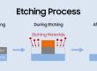
6. Etching
Types:
Wet Chemical Etching:
Uses liquid etchants (e.g., HNO₃ for metals, KOH for silicon).
Pros: Low cost, high throughput, no thermal stress.
Cons: Isotropic etching (undercut), limited aspect ratios.
Dry (Plasma) Etching:
Uses ionized gas (e.g., reactive ion etching/RIE).
Pros: Anisotropic profiles, high precision, sub-micron resolution.
Cons: Expensive equipment, slower than wet etching.
Pros:
No mechanical stress or tool wear.
Ideal for ultra-thin materials (<0.1 mm).
Batch processing of thousands of holes simultaneously.
Cons:
Limited to materials with selective etchants.
Mask alignment critical for accuracy.
Applications:
Semiconductor vias, MEMS devices, microfluidic channels, stencils.
Decision-Making Framework (Revised)
Material Conductive?
Yes → EDM, ECM, wet etching (metals).
No → Laser, plasma etching (glass, ceramics, polymers).
Hole Diameter <0.1 mm?
Yes → Laser/EDM/plasma etching.
High Aspect Ratio?
Yes → ECM/plasma etching (dry).
Batch Production?
Yes → Photochemical etching.
Edge Precision Critical?
Yes → Dry etching; No → Wet etching.
Case Studies (Added Etching Examples)
Electronics: Photochemical etching of stainless steel sieves (0.05 mm holes, 10,000+ holes per batch).
Medical: Plasma-etched polymer microfluidic chips (0.03 mm channels, 10:1 aspect ratio).
Semiconductors: Deep reactive ion etching (DRIE) for silicon vias in 3D ICs (0.02 mm, 15:1 aspect ratio).
Emerging Trends
Nanoscale Etching: Atomic layer etching (ALE) for sub-10 nm features.
Hybrid Laser-Etching: Laser pre-drilling followed by etching for high-aspect-ratio holes.
Conclusion
Etching expands the toolkit for micro hole machining, particularly for non-conductive materials, ultra-thin substrates, and high-throughput applications. Wet etching suits cost-sensitive bulk production, while plasma etching enables nanoscale precision. When combined with traditional methods like laser or EDM, etching bridges gaps in complexity, scalability, and material compatibility.
Appendix: Updated Comparison Table
| Method | Min Diameter (mm) | Aspect Ratio | Tolerance (±mm) | Surface Finish (Ra µm) | Materials | Cost Efficiency |
|---|---|---|---|---|---|---|
| Mechanical | 0.05 | Up to 10:1 | 0.005 | 0.5–1.5 | All | High volume |
| Laser | 0.01 | Up to 30:1 | 0.01 | 1–2 | Most | Low/medium volume |
| EDM | 0.02 | Up to 20:1 | 0.005 | 0.2–0.4 | Conductive | Medium volume |
| ECM | 0.05 | Up to 50:1 | 0.005 | 0.1 | Conductive | High volume |
| Ultrasonic | 0.1 | Up to 5:1 | 0.02 | 0.5–1 | Brittle | Low volume |
| Wet Etching | 0.02 | 1:1–3:1 | 0.01 | 0.3–0.8 | Metals, Glass, Polymers | High volume (batch) |
| Dry Etching | 0.01 | Up to 20:1 | 0.005 | 0.1–0.5 | Silicon, Ceramics | Medium/high volume |
This guide equips engineers to navigate micro hole machining complexities, ensuring optimal outcomes across industries. Etching methods now provide critical solutions for semiconductor, biomedical, and precision manufacturing challenges.

- Etching Cost Calculator - June 14, 2026
- Surface Area Calculator - May 24, 2026
- Etch Rate Calculator - May 24, 2026