1. Introduction
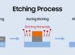
Etching is a critical manufacturing process used to selectively remove material from substrates, particularly in semiconductor fabrication, microelectromechanical systems (MEMS), and printed circuit boards (PCBs). The speed of etching, or etch rate, directly impacts process efficiency, precision, and final product quality. This article explores the role of etching speed, its influencing factors, and its implications across industries.
2. Basics of Etching
Etching involves two primary methods:
Wet Etching: Uses liquid chemicals (e.g., acids) to dissolve materials. It is isotropic, etching uniformly in all directions.
Dry Etching: Employs plasma or reactive ions (e.g., reactive ion etching, RIE) for anisotropic etching, enabling vertical sidewalls.
Etching Speed Definition: The rate of material removal, measured in nm/min or µm/min. It is influenced by etchant chemistry, temperature, plasma parameters, and material properties.
3. Factors Influencing Etching Speed
Chemical Concentration & Reactivity: Higher concentrations or reactive species (e.g., Cl₂ in plasma) accelerate etching.
Temperature: Elevated temperatures increase reaction kinetics but may compromise mask integrity.
Plasma Parameters: In dry etching, ion energy, gas flow rates, and RF power modulate etch rates.
Material Properties: Crystallinity and bond strength affect susceptibility to etching (e.g., silicon vs. silicon dioxide).
4. Impact of Etching Speed on the Process
a. Precision and Feature Resolution
High Speed: Risks over-etching, undercutting, and loss of critical dimensions, especially in nanoscale semiconductor features.
Low Speed: Enhances control for high-aspect-ratio structures (e.g., MEMS trenches) but reduces throughput.
b. Surface Morphology
Rapid etching may induce surface roughness due to uneven material removal, impacting electrical performance in devices.
c. Selectivity
High etch rates can reduce selectivity, eroding masking layers (e.g., photoresist) or underlying materials.
d. Uniformity
Non-uniform etch rates cause inconsistencies, particularly in large-area substrates, due to etchant depletion or plasma inhomogeneity.
e. Throughput vs. Quality Trade-off
Faster etching boosts production rates but may increase defects; slower processes favor precision at higher costs.
5. Industry-Specific Applications
Semiconductors: Precise etch rates are vital for transistor gate etching. For example, over-etching in FinFETs can alter electrical characteristics.
MEMS: Deep reactive ion etching (DRIE) balances speed and anisotropy to create high-aspect-ratio structures.
PCB Manufacturing: Controlled copper etching ensures trace integrity while maintaining production efficiency.
6. Optimization Strategies
Parameter Tuning: Adjusting plasma power, gas mixtures, or etchant concentration to balance speed and quality.
Advanced Techniques: Pulse-modulated plasma or cryogenic etching reduces damage while maintaining rates.
In-Situ Monitoring: Optical emission spectroscopy (OES) or interferometry enables real-time adjustments.
7. Challenges and Trade-offs
Defect Formation: High-speed processes may introduce microtrenches or residue.
Material Compatibility: Aggressive etchants risk damaging sensitive layers (e.g., low-κ dielectrics).
Cost Considerations: Slow etching increases operational expenses, necessitating a cost-quality balance.
8. Future Trends
Atomic Layer Etching (ALE): Layer-by-layer removal for atomic-level precision, albeit slower.
AI-Driven Process Control: Machine learning algorithms optimize etch parameters dynamically.
Green Etching: Developing eco-friendly etchants with comparable performance.
9. Case Study: Silicon Wafer Etching
A study comparing SF₆/O₂ plasma ratios in RIE showed that higher SF₆ concentrations increased etch rates but reduced anisotropy due to radical-driven etching. Optimizing gas ratios achieved a 500 nm/min rate with vertical sidewalls, critical for 5-nm node semiconductor devices.
10. Conclusion
Etching speed is a pivotal factor influencing manufacturing outcomes across industries. Balancing speed with precision, selectivity, and uniformity remains a key challenge. Advances in process monitoring and novel techniques promise to enhance control, enabling faster yet higher-quality etching for next-generation technologies.

- Etching Cost Calculator - June 14, 2026
- Surface Area Calculator - May 24, 2026
- Etch Rate Calculator - May 24, 2026