Precision etching is a cornerstone of microfabrication, essential in industries like semiconductors, microelectronics, and MEMS. Achieving high accuracy in etching requires meticulous preparation, with surface preparation emerging as the most critical step. This article explores why thorough surface cleaning and conditioning are indispensable before initiating precision etching.
1. Understanding Precision Etching
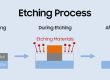
Precision etching involves selectively removing material to create intricate patterns, typically using chemical (wet) or plasma (dry) methods. Applications range from integrated circuits to medical devices. The process relies on photolithography to transfer a design onto a substrate via a photoresist mask, which protects areas from the etchant.
2. The Primacy of Surface Preparation
Before etching, the substrate must undergo rigorous surface preparation, primarily cleaning, to eliminate contaminants. Here’s why this step is paramount:
2.1. Contaminant Removal
Organic Residues: Oils, dust, or fingerprints disrupt photoresist adhesion, causing delamination during etching.
Particles: Even sub-micron particles create defects, leading to circuit shorts or opens.
Oxides/Native Layers: Unremoved oxide layers (e.g., on silicon) alter etch rates and uniformity.
2.2. Adhesion Promotion
Hydrophobic Surfaces: Materials like silicon become hydrophobic when oxidized. Cleaning with solutions like piranha (H₂SO₄ + H₂O₂) or oxygen plasma renders surfaces hydrophilic, ensuring photoresist adherence.
Adhesion Layers: Metals like titanium or chromium are often sputtered onto substrates (e.g., glass) to enhance resist bonding.
2.3. Etch Uniformity
Contaminants cause localized variations in etch rates, leading to undercutting or incomplete etching. A pristine surface ensures consistent material removal.
3. Surface Preparation Techniques
3.1. Wet Cleaning
RCA Clean: A two-step process for silicon wafers:
SC-1 (Ammonia-Peroxide): Removes organic contaminants.
SC-2 (Hydrochloric Acid-Peroxide): Eliminates metallic ions.
Piranha Etch: Removes stubborn organic residues but requires careful handling.
3.2. Dry Cleaning
Plasma Ashing: Oxygen plasma oxidizes organic contaminants.
UV-Ozone Treatment: Breaks down hydrocarbons via ultraviolet light and ozone.
3.3. Mechanical Methods
CMP (Chemical Mechanical Planarization): Polishes surfaces to nanometer-level flatness for advanced nodes.
4. Secondary Preparatory Steps
While surface preparation is foundational, other steps are also crucial:
4.1. Photomask Design and Alignment
Design for Etch (DFE): Compensates for etch biases (e.g., isotropic undercut).
Alignment Marks: Ensure precise overlay in multi-layer devices.
4.2. Photoresist Application
Spin Coating: Achieves uniform resist thickness.
Soft Baking: Removes solvents to stabilize the resist.
4.3. Process Parameter Calibration
Etch Rate Calibration: Determines time/temperature for target depth.
Selectivity Testing: Ensures the etchant attacks the substrate, not the resist.
5. Consequences of Poor Surface Preparation
Resist Delamination: Causes unintended etching and pattern distortion.
Microscopic Defects: Particles create pinholes, leading to electrical failures.
Yield Loss: Up to 50% of wafer defects stem from improper cleaning.
6. Case Study: Semiconductor Wafer Fabrication
In semiconductor fabs, wafers undergo:
Pre-Clean: RCA or piranha treatment.
Adhesion Promotion: Hexamethyldisilazane (HMDS) primes the surface.
Photolithography: Resist spin-coating, exposure, and development.
A single particle >0.1µm can ruin a die, highlighting the need for ISO Class 1 cleanrooms.
7. Conclusion
While photomask accuracy and etch parameters are vital, surface preparation—particularly cleaning—is the linchpin of precision etching. A contaminant-free substrate ensures photoresist adhesion, etch uniformity, and defect-free patterning. Neglecting this step compromises the entire process, underscoring its status as the foremost prerequisite in precision etching.
Best Practices:
Implement rigorous cleaning protocols (RCA, plasma).
Monitor cleanliness via AFM or ellipsometry.
Integrate inline metrology for real-time defect detection.
By prioritizing surface preparation, manufacturers achieve the fidelity required for next-generation microdevices.

- Etching Cost Calculator - June 14, 2026
- Surface Area Calculator - May 24, 2026
- Etch Rate Calculator - May 24, 2026