Stencil etching is a microfabrication technique that employs a physical mask (stencil) to selectively remove material from a substrate. Unlike photolithography, which uses light-sensitive resists, stencil etching relies on direct patterning, offering unique benefits across industries. This article explores the key advantages of stencil etching, emphasizing its efficiency, versatility, and cost-effectiveness.
1. Cost-Effectiveness
Stencil etching reduces production costs significantly. Reusable stencils, especially those made from durable materials like stainless steel or nickel, lower expenses over time compared to single-use photomasks. The elimination of photoresist chemicals, developers, and associated equipment further cuts material and operational costs, making it ideal for budget-conscious projects.
2. Process Simplicity and Speed
By bypassing photoresist coating, exposure, and development steps, stencil etching streamlines fabrication. The direct application of the stencil onto the substrate allows immediate etching, accelerating production cycles. This simplicity is advantageous for rapid prototyping and high-throughput manufacturing.
3. Material and Substrate Versatility
Stencil etching accommodates diverse materials, including sensitive substrates like polymers, textiles, and non-planar surfaces. Unlike photolithography, which requires specific resist adhesion, stencils can be tailored to withstand aggressive etchants (e.g., acids, plasmas), enabling compatibility with metals, ceramics, and composites.
4. Environmental Benefits
Reduced reliance on toxic photoresists and solvents minimizes hazardous waste. Stencil etching aligns with green manufacturing initiatives by lowering chemical consumption and disposal costs, appealing to industries prioritizing sustainability.
5. Scalability
Suitable for both small-scale custom jobs and large-scale production, stencil etching offers flexibility. Laser-cut or electroformed stencils maintain precision across batches, while quick design modifications support iterative development without costly mask redesigns.
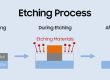
6. Thicker Etch Depths
Durable stencils withstand prolonged etching, enabling deeper features—critical for MEMS, microfluidics, and PCB manufacturing. Unlike photoresists, which may degrade, metal stencils ensure consistent performance in deep etching applications.
7. Reduced Contamination
The absence of photoresist eliminates post-etch cleaning steps, reducing residue-related defects. This is crucial for optical or electronic components where surface purity is paramount.
8. Design Flexibility
Stencils are easily redesigned using CAD and fabricated via laser cutting or electroforming. This adaptability supports custom patterns and iterative testing, ideal for R&D and niche applications.
9. No Cleanroom Dependency
Stencil etching can be performed in standard laboratory environments, bypassing the need for expensive cleanroom facilities. This accessibility democratizes microfabrication for smaller labs and educational institutions.
Applications and Use Cases
Flexible Electronics: Stencil etching patterns conductive inks on bendable substrates.
MEMS/NEMS: Creates high-aspect-ratio structures without resist limitations.
Art and Jewelry: Enables intricate designs on metals and polymers.
Aerospace: Etches lightweight, durable components for sensors and panels.
Conclusion
Stencil etching emerges as a versatile, economical alternative to traditional lithography. Its advantages—cost savings, speed, material flexibility, and environmental benefits—make it indispensable in industries ranging from electronics to art. While resolution limits may restrict its use in sub-micron applications, ongoing advancements in stencil fabrication promise broader adoption. For projects prioritizing efficiency and adaptability, stencil etching stands out as a compelling solution.

- Etching Cost Calculator - June 14, 2026
- Surface Area Calculator - May 24, 2026
- Etch Rate Calculator - May 24, 2026