Chemical etching, also known as photochemical machining (PCM), is a subtractive manufacturing process used to produce intricate metal components with high precision. It involves selectively removing material using chemical reactions, guided by a photoresist mask. While the process offers advantages like no mechanical stress and cost-effective prototyping, achieving tight dimensional tolerances remains challenging. This article explores the key factors affecting dimensional control in chemical etching and strategies to mitigate them.
1. Undercutting and Isotropic Etching
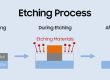
Issue: Chemical etchants typically act isotropically, removing material uniformly in all directions. This leads to undercutting—lateral etching beneath the photoresist mask—resulting in features wider than designed. The etch factor (ratio of etch depth to undercut) determines severity; a low etch factor exacerbates dimensional inaccuracies.
Impact:
- Tapered sidewalls instead of vertical edges.
- Over-sizing of features, critical for high-precision parts like microfluidic channels or electrical contacts.
Mitigation:
- Use etchants with improved anisotropy (e.g., doped acids).
- Compensate mask designs by reducing feature sizes to account for undercut.
- Optimize etch time to minimize over-etching.
2. Process Parameter Variability
Key Parameters:
- Etchant Concentration and Temperature: Higher temperatures accelerate etching, risking loss of control. Concentration depletion over time reduces consistency.
- Agitation: Poor agitation causes etchant stagnation, leading to uneven material removal.
- Time: Over-etching enlarges features; under-etching leaves residual material.
Impact:
- Batch-to-batch inconsistencies.
- Non-uniform etching depths in complex geometries.
Mitigation:
- Automated monitoring systems for real-time adjustment of temperature and concentration.
- Regular etchant replenishment and filtration to remove byproducts.
- Precise timing controls with endpoint detection (e.g., weight or thickness sensors).
3. Material-Related Challenges
Factors:
- Thickness Variations: Non-uniform stock material leads to partial etching in thicker areas.
- Grain Structure and Alloy Composition: Inhomogeneous materials etch unevenly; impurities cause pitting.
- Resist Adhesion: Poor adhesion results in etchant seepage and feature distortion.
Impact:
- Variable etch rates across a single part.
- Surface roughness affecting functional dimensions.
Mitigation:
- Source materials with tight thickness tolerances and homogeneous microstructure.
- Pre-etch surface treatments (e.g., cleaning, passivation).
- High-resolution photoresists with strong adhesion (e.g., dry-film resists).
4. Photolithography Limitations
Issues:
- Mask Alignment Errors: Misalignment during UV exposure shifts features.
- Photoresist Resolution: Low-resolution resists blur fine details, enlarging features.
- Development Defects: Incomplete resist removal leaves artifacts.
Impact:
- Misregistered features (e.g., misaligned holes in PCBs).
- Loss of critical dimensions in sub-millimeter features.
Mitigation:
- High-precision alignment systems (e.g., laser-guided).
- Advanced resists with <10 µm resolution (e.g., liquid photopolymers).
- Robust development processes with controlled spray parameters.
5. Environmental and Post-Process Factors
Issues:
- Ambient Conditions: Humidity/temperature fluctuations affect resist coating and drying.
- Rinsing and Drying: Residual etchant continues reacting; thermal drying warps thin parts.
Impact:
- Post-etch corrosion or warpage.
- Delamination of resist during processing.
Mitigation:
- Climate-controlled production environments.
- Neutralizing baths post-etch and air-knife drying.
6. Design and Metrology Considerations
Issues:
- Aspect Ratio Limits: High depth-to-width ratios hinder etchant access, causing incomplete etching.
- Tolerance Stacking: Cumulative errors from mask design, resist application, and etching.
Impact:
- Tapered profiles in deep channels or cavities.
- Rejected parts due to exceeded tolerances.
Mitigation:
- Design rules limiting aspect ratios (typically <3:1 for chemical etching).
- Statistical process control (SPC) to track error sources.
- High-accuracy metrology tools (e.g., optical comparators, CMMs).
Conclusion
Dimensional control in chemical etching hinges on managing isotropic etching effects, process parameters, material consistency, and photolithographic precision. Advances in process automation, material science, and mask design software (e.g., CAD compensation algorithms) continue to enhance accuracy. By integrating robust quality control measures and understanding the interplay of factors discussed, manufacturers can achieve tolerances as tight as ±10% of material thickness, making chemical etching viable for aerospace, electronics, and medical device industries.

- Etching Cost Calculator - June 14, 2026
- Surface Area Calculator - May 24, 2026
- Etch Rate Calculator - May 24, 2026