Metal etching is a critical process in industries ranging from electronics to aerospace, enabling precise patterning of metal components. A key element of this process is the photosensitive anti-corrosion layer , which protects selected areas of the metal from corrosive etchants. This guide explores the materials, methods, and best practices for creating such a layer, ensuring high precision and durability.
1. Understanding the Photosensitive Anti-Corrosion Layer
The photosensitive layer, or photoresist, serves two primary functions:
- Photosensitivity: Reacts to UV light to form a patterned mask.
- Anti-corrosion: Resists chemical etchants (e.g., acids, alkalis) during the etching process.
Types of Photoresists
- Negative Photoresists
- Harden upon UV exposure, becoming insoluble.
- Ideal for high-resolution patterns (e.g., AZ-1500 series, SU-8).
- Positive Photoresists
- Exposed areas become soluble.
- Used for fine features (e.g., S1813, PMMA).
Material Selection Criteria:
- Compatibility with the metal substrate (copper, aluminum, steel).
- Resistance to the etchant (e.g., ferric chloride for copper, HNO₃ for aluminum).
- Adhesion strength and resolution requirements.
2. Process Steps for Applying the Photosensitive Layer
Step 1: Surface Preparation
Goal: Ensure optimal adhesion by removing contaminants.
- Cleaning: Degrease with acetone or isopropyl alcohol.
- Mechanical Abrasion: Use pumice or sandblasting for rough metals.
- Chemical Treatment: Acid pickling (e.g., HCl for steel) to remove oxides.
Step 2: Photoresist Application
Methods:
- Spin Coating: For flat, small substrates (1,000–3,000 RPM).
- Spray Coating: For complex geometries; ensures uniform thickness.
- Dry Film Lamination: Pre-made films heated and pressed onto the metal (common in PCB manufacturing).
Thickness: Typically 1–25 µm, adjusted via viscosity or application speed.
Step 3: Pre-Bake (Soft Bake)
- Removes solvents from the photoresist.
- Temperature: 90–100°C for 5–15 minutes (varies by resist type).
Step 4: UV Exposure
- Equipment: Collimated UV light source (350–450 nm wavelength).
- Photomask: High-contrast film or glass mask with the desired pattern.
- Exposure Time: 10–60 seconds (determined by resist datasheet).
Step 5: Development
- Negative Resists: Unexposed areas dissolve in developer (e.g., TMAH for SU-8).
- Positive Resists: Exposed areas dissolve (e.g., KOH-based developers).
- Rinse: Deionized water to halt development.
Step 6: Post-Bake (Hard Bake)
- Enhances chemical resistance.
- Temperature: 120–150°C for 10–30 minutes.
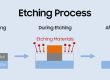
3. Etching and Post-Processing
Etching Process
- Common Etchants:
- Copper: FeCl₃, ammonium persulfate.
- Aluminum: HNO₃, NaOH.
- Stainless Steel : HCl/HNO₃ mixture.
- Monitoring : Etch time varies with temperature and concentration.
Stripping the Photoresist
- Solvents: Acetone or proprietary strippers (e.g., NMP for tough resists).
- Eco-Friendly Options: Bio-based solvents or alkaline solutions.
Neutralization and Finishing
- Neutralize residual etchant (e.g., baking soda for acids).
- Apply protective coatings (e.g. , passivation for stainless steel) .
4. Advanced Techniques and Innovations
- Laser Direct Imaging (LDI): Skips photomasks by using lasers for higher precision.
- Electrodeposited Photoresists: Uniform layers for complex shapes.
- Bio-Based Resists: Environmentally friendly options (e.g., starch derivatives).
5. Troubleshooting Common Issues
| Issue | Cause | Solution |
|---|---|---|
| Poor Adhesion | Contaminated surface | Improve cleaning/abrasion steps. |
| Undercutting | Over-etching or weak resist | Optimize etch time; use higher-resist. |
| Incomplete Development | Insufficient exposure/developer | Calibrate exposure time; fresh developer. |
6. Safety and Environmental Considerations
- Ventilation: Use fume hoods for etching and stripping.
- Waste Disposal: Neutralize acids/bases before disposal.
- PPE: Gloves, goggles, and aprons when handling chemicals.
7. Applications
- Electronics: PCB trace patterning.
- Aerospace: Lightweight component fabrication.
- Art and Jewelry: Detailed decorative designs.
Conclusion
Creating a photosensitive anti-corrosion layer involves meticulous material selection, precise process control, and adherence to safety protocols. Advances in photoresist technology continue to enhance resolution and sustainability, making metal etching more efficient and eco-friendly. By following this guide, manufacturers can achieve high-quality, corrosion-resistant patterns tailored to diverse industrial needs.

- Etching Cost Calculator - June 14, 2026
- Surface Area Calculator - May 24, 2026
- Etch Rate Calculator - May 24, 2026