Circuit board etching is a critical step in PCB manufacturing, involving the removal of excess copper to create conductive pathways. This guide explores various etching techniques, from traditional chemical methods to modern mechanical processes, providing insights into their applications, advantages, and limitations.
1. Chemical Etching Methods
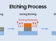
Chemical etching uses reactive solutions to dissolve unprotected copper. Key steps include applying a resist, etching, and cleaning.
1.1 Ferric Chloride (FeCl₃)
Process: Apply resist (toner, photoresist), immerse in FeCl₃, agitate until copper dissolves.
Pros: Widely available, effective for most projects.
Cons: Messy, stains surfaces, disposal challenges.
Safety: Use gloves/eye protection; neutralize with baking soda before disposal.
1.2 Ammonium Persulfate
Process: Dissolve crystals in water, etch at 40–50°C.
Pros: Clear solution allows monitoring, less residue.
Cons: Slower than FeCl₃, degrades over time.
Use Case: High-precision boards requiring visual inspection.
1.3 Hydrochloric Acid + Hydrogen Peroxide (HCl/H₂O₂)
Process: Mix HCl and H₂O₂ (3:1 ratio), etch rapidly.
Pros: Fast, reusable with H₂O₂ replenishment.
Cons: Hazardous fumes; requires careful handling.
Tip: Neutralize with sodium bicarbonate post-use.
1.4 Citric Acid-Based Etchants
Process: Mix citric acid, hydrogen peroxide, and water.
Pros: Eco-friendly, safe disposal.
Cons: Slower, shorter shelf life.
Ideal For: Hobbyists prioritizing safety.
1.5 Electrochemical Etching
Process: Submerge PCB in saltwater, apply current (PCB as anode).
Pros: Reusable electrolyte, controlled etching.
Cons: Requires power supply, slower for thick copper.
2. Physical/Mechanical Methods
These methods remove copper without chemicals, ideal for rapid prototyping.
2.1 CNC Milling
Process: Use a CNC machine with a carbide bit to mill away copper.
Pros: No chemicals, instant drilling/routing.
Cons: Limited resolution, tool wear, noise.
Use Case: Low-volume prototypes.
2.2 Laser Etching
Process: Ablate copper with a high-power laser.
Pros: High precision, no masks/resists.
Cons: Expensive equipment, slow for large boards.
Applications: Industrial high-density interconnects.
3. Photolithographic Techniques
Combine chemical and UV processes for high accuracy.
3.1 Dry Film Photoresist
Process: Laminate UV-sensitive film, expose via mask, develop, etch.
Pros: High resolution, durable resist.
Cons: Requires UV exposure unit.
3.2 Liquid Photoresist
Process: Spin-coat liquid resist, expose, develop.
Pros: Finer traces, flexibility.
Cons: Messy application.
4. Alternative Methods
4.1 Toner Transfer
Process : Print design on glossy paper, iron onto PCB, etch.
Pros: Low cost, simple.
Cons: Moderate resolution, paper removal challenges.
4.2 Vinyl Masking
Process: Cut design on vinyl cutter, adhere to PCB, etch.
Pros: No printer needed, reusable stencils.
Cons: Limited detail.
5. Safety and Environmental Considerations
Ventilation: Essential for chemical methods to avoid inhaling fumes.
Disposal: Neutralize acidic/basic etchants; avoid draining metals.
PPE: Gloves, goggles, and aprons mandatory.
6. Method Comparison
| Method | Cost | Precision | Speed | Safety |
|---|---|---|---|---|
| Ferric Chloride | Low | Moderate | Moderate | Moderate risk |
| CNC Milling | High | High | Fast | Safe |
| Photolithography | Medium | Very High | Slow | Low risk |
| Toner Transfer | Very Low | Low | Fast | Low risk |
Conclusion
Choosing an etching method depends on precision needs, budget, and safety preferences. Chemical methods like ferric chloride suit hobbyists, while photolithography offers industrial precision. Mechanical methods like CNC milling provide quick, chemical-free results. Always prioritize safety and environmental guidelines to ensure sustainable practices.

- Etching Cost Calculator - June 14, 2026
- Surface Area Calculator - May 24, 2026
- Etch Rate Calculator - May 24, 2026