Copper chemical etching is a subtractive manufacturing process that selectively removes copper from a substrate using chemical solutions. Widely used in electronics, aerospace, and decorative arts, this technique enables precise patterning without mechanical stress. This article explores the key characteristics, processes, applications, and considerations of copper chemical etching.
1. Etching Process Overview
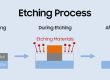
The process involves:
Cleaning: Removing contaminants to ensure uniform etching.
Resist Application: Applying a protective layer (photoresist, polymer, or wax) to mask desired areas.
Exposure and Development: Transferring patterns via UV light (photolithography) or direct masking.
Etching: Immersing the substrate in an etchant to dissolve exposed copper.
Resist Removal: Stripping the resist to reveal the final design.
2. Key Characteristics of Copper Chemical Etching
2.1 Etchants and Their Properties
Common etchants include:
Ferric Chloride (FeCl₃): Cost-effective and widely used but generates hazardous waste.
Cupric Chloride (CuCl₂): Regenerable with HCl and O₂, preferred for industrial scalability.
Ammonium Persulfate ((NH₄)₂S₂O₈): Less toxic, produces smoother finishes.
Nitric Acid (HNO₃) : Fast etching but highly corrosive and hazardous.
2.2 Etch Rate
Influenced by:
Concentration: Higher concentrations accelerate etching but may compromise resist integrity.
Temperature: Elevated temperatures increase reaction speed (e.g., FeCl₃ at 40–50°C etches ~25 µm/min).
Agitation: Enhances etchant circulation, preventing stagnation and ensuring consistent rates.
2.3 Resolution and Undercut
Resolution: The minimum feature size achievable (typically 25–50 µm). Depends on resist quality and etch control.
Undercut: Lateral etching beneath the resist, causing feature widening. Mitigated by optimizing etchant selectivity and using thicker resists. Isotropic etching (equal material removal in all directions) is inherent in chemical methods.
2.4 Surface Finish
Etchants like ammonium persulfate yield smoother surfaces, critical for PCB conductivity.
Roughness increases with aggressive etchants (e.g., FeCl₃), necessitating post-etch polishing.
3. Applications
Electronics: PCB fabrication for circuitry and antennas.
MEMS: Precision components in sensors and actuators.
Decorative Arts: Intricate designs in jewelry and signage.
EMI Shielding: Thin copper layers for electromagnetic interference protection.
4. Advantages and Disadvantages
Pros:
No mechanical stress, ideal for delicate structures.
High scalability and complex pattern replication.
Cost-effective for mass production.
Cons:
Chemical handling and waste disposal challenges.
Limited anisotropy leading to undercut.
5. Environmental and Safety Considerations
Waste Management: Neutralization of acidic etchants (e.g., FeCl₃ with NaOH) and recycling (CuCl₂ regeneration).
Safety Protocols: PPE (gloves, goggles), fume hoods, and spill containment measures.
Eco-Friendly Trends: Development of biodegradable etchants and closed-loop systems.
6. Future Trends
Nanotechnology: Ultra-high-resolution etching for nanoelectronics.
Green Chemistry: Non-toxic etchants (e.g., citric acid-based solutions).
Automation: AI-driven process control for precision and waste reduction.
Conclusion
Copper chemical etching balances precision, scalability, and versatility, making it indispensable across industries. Understanding its characteristics—etchant selection, resolution limits, and environmental impact—enables optimization for specific applications. As technology advances, sustainable practices and innovation will drive its evolution, ensuring relevance in modern manufacturing.

- Etching Cost Calculator - June 14, 2026
- Surface Area Calculator - May 24, 2026
- Etch Rate Calculator - May 24, 2026