In the intricate world of modern manufacturing, particularly for electronics, sensors, medical devices, and precision engineering, the demand for complex, miniaturized, and burr-free metal components is ever-increasing. Metal Mask Etching Processing (also known as Photochemical Machining, PCM, or Chemical Etching) has emerged as a vital subtractive manufacturing technique that excels where traditional methods falter. This process uses controlled chemical reactions, guided by precisely patterned photoresist masks, to selectively dissolve metal, transforming flat sheets into intricate parts. Let’s delve into the significant advantages that make metal mask etching a preferred choice.
Key Advantages of Metal Mask Etching Processing:
Exceptional Precision and Complexity:
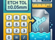
Micro-Scale Features: Etching achieves remarkably fine details, routinely producing features (lines, holes, slots) down to 0.025mm (0.001 inches) and tolerances as tight as ±10% of material thickness. This is crucial for components like lead frames, fine meshes, RF/EMI shields, and sensor elements.
Intricate Geometries: The process effortlessly handles complex internal and external shapes, sharp corners, and delicate patterns that would be extremely difficult, expensive, or impossible to achieve via punching, stamping, or laser cutting without distortion or tooling limitations.
Simultaneous Two-Sided Etching: Complex patterns can be etched identically on both sides of the sheet simultaneously with perfect registration, essential for components like electrical contacts and encoder disks.
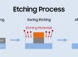
Burr-Free and Stress-Free Components:
No Mechanical Stress: Unlike stamping, punching, or machining, etching involves no cutting forces, pressure, or heat (during material removal). This eliminates work hardening, mechanical stresses, micro-cracks, and deformation, preserving the metal’s original properties (grain structure, magnetic properties, temper).
Perfectly Smooth Edges: The chemical dissolution process inherently produces parts with perfectly smooth, clean, and burr-free edges. This is critical for:
Electrical contacts (prevents arcing/shorting)
Cutting tools (razor blades, surgical instruments)
Fluidic components (prevents turbulence/contamination)
Assembly (prevents scratching, ensures proper fit)
No Heat-Affected Zone (HAZ):
Since material removal occurs chemically at ambient temperatures, there is absolutely no Heat-Affected Zone (HAZ). This is a major advantage over laser cutting, EDM, or plasma cutting.
Benefits: Preserves temper and hardness of heat-treated materials (spring steels, beryllium copper), prevents thermal distortion/warping, avoids changes in magnetic properties (important for electrical steels), and maintains material corrosion resistance.
Design Flexibility & Rapid Prototyping:
Low-Cost Tooling: The “tool” is a digital phototool (film or glass mask). Creating or modifying these is significantly faster and cheaper (often 10-20% of the cost) than producing hard tooling (stamping dies, molds).
Fast Iterations: Design changes are implemented simply by modifying the digital artwork and producing a new phototool, enabling extremely rapid prototyping and design iteration cycles (days vs. weeks/months for hard tooling).
No Design Limitations: Complexities like overlapping features, varying densities, or nested parts don’t increase processing difficulty or cost significantly, as they would with mechanical tooling.
Material Versatility:
Etching works effectively with a vast range of metals and alloys, including:
Copper & Alloys: C110, C194, C260 (Brass), C510 (Phos Bronze), Beryllium Copper.
Stainless Steels: 304, 316, 17-7PH, 301, 430.
Nickel & Alloys: Nickel 200/201, Inconel 600/625, Monel 400, Kovar.
Aluminum: Various alloys (requires specialized chemistry).
Titanium & Alloys: CP grades, Ti-6Al-4V.
Specialty Alloys: Molybdenum, Tungsten, Elgiloy, Nitinol (Shape Memory).
Material Property Preservation: As mentioned, the cold process preserves temper, hardness, magnetic properties, and corrosion resistance inherent to the raw material.
Cost-Effectiveness for Specific Scenarios:
Low-Volume & Prototypes: Extremely cost-effective for prototypes, R&D, and low-to-medium volume production due to minimal tooling investment.
High Complexity: For parts with extreme complexity or fine features, etching often becomes more economical than machining or stamping, where tool wear or complexity drives costs prohibitively high.
Thin Materials: Highly efficient and precise for processing thin foils and sheets (down to 0.010mm / 0.0004″) where stamping or laser cutting struggle with distortion or heat damage.
Reduced Secondary Operations: Burr-free, clean edges often eliminate the need for costly secondary deburring, cleaning, or finishing operations required by other processes.
High Consistency and Repeatability:
Once the process parameters (chemistry, time, temperature) are optimized for a specific material and design, etching provides exceptional consistency and repeatability across large production runs. Digital phototools ensure each part is identical.
Cleanliness and Surface Finish:
The process produces parts free from oils, coolants, or residues associated with machining or stamping. A consistent, matte surface finish is typical, which can be advantageous for subsequent plating, painting, or bonding. Selective etching can also create specific surface textures.
Limitations to Consider (For Balance):
Material Thickness: Primarily suited for thin to medium sheet/foil (typically 0.010mm to 2.0mm, up to ~3.0mm for some metals/alloys). Thicker materials require impractical etching times.
Etch Factor: Chemical etching is isotropic, meaning it etches sideways (“undercut”) at a predictable rate relative to the depth. This “etch factor” must be accounted for in the phototool design.
Environmental Considerations: Requires handling and disposal of chemical etchants and rinse waters according to strict environmental regulations. Modern facilities employ advanced recycling and treatment systems.
Feature Size vs. Thickness Ratio: Very deep, narrow holes or channels can be challenging due to the etch factor limiting aspect ratios.
Conclusion:
Metal Mask Etching Processing stands out as an indispensable manufacturing technique, offering a unique combination of precision, complexity, stress-free production, burr-free edges, and design flexibility unmatched by many traditional methods. Its ability to handle a wide range of materials without inducing thermal damage or mechanical stress makes it particularly valuable for sensitive applications in electronics, medical devices, aerospace, and filtration. While material thickness imposes a natural limit, the advantages of rapid prototyping, low-cost tooling for complex parts, and consistent high quality solidify etching’s role as a cornerstone technology for producing the intricate, high-performance metal components demanded by modern industry. When complexity, precision, and material integrity are paramount, photochemical etching is often the optimal solution.

- Etching Cost Calculator - June 14, 2026
- Surface Area Calculator - May 24, 2026
- Etch Rate Calculator - May 24, 2026